A GLOBAL LEADER
Products
Introduction
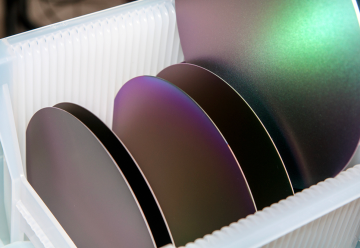
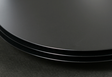
As the world’s leading silicon wafer (a substrate for integrated circuits) manufacturer, the Shin-Etsu Group continues to run at the leading edge of high-flatness and larger diameters in its wafer products. It has met early success with strong sales of its next-generation 300mm-diameter wafers and Silicon On Insulator wafers.
Typical materials supplied to our customers are as follows:
We will assess the specification, once we receive your detailed enquiry. You can make a product enquiry by emailing [email protected]
Crystal
Crystal Types
CZ
Boron (B)
Phosphorous (P)
Antimony (Sb)
Arsenic (As)
Red Phosphorous
FZ
Boron (B)
Phosphorous (P)
Neutron Transmutation Doping (NTD)
Diameter
Diameter Selection typically
150mm through 300mm
others may be available.
Please ask
Orientation selection
< 100 >
< 111 >
< 110 >
< 511 >
Final Product
Polished Wafer (PW)
Epitaxial Wafer (EPI)
Annealed Wafer
Diffused Wafer (DW)
Non-polished Wafer (NPW)
Silicon On Insulator (SOI)
Shin-Etsu Handotai Europe Ltd, Registered in Scotland No: SC087947
Address